
Engineered for laboratory research, semiconductor quality assurance, BMS validation, and automated production testing lines.
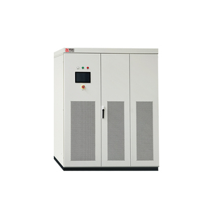
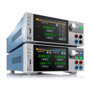
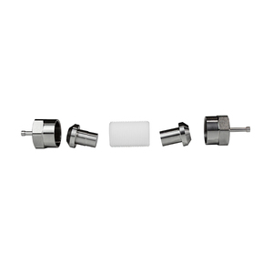
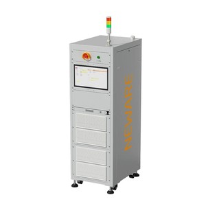
As global power electronics rapidly transition from legacy Silicon (Si) MOSFETs and IGBTs toward Wide-Bandgap (WBG) materials, Gallium Nitride (GaN) High Electron Mobility Transistors (HEMTs) have established dominance in high-frequency, high-efficiency power conversion. Operating at switching frequencies exceeding megahertz (MHz) thresholds and delivering switching speeds ($dv/dt$) in excess of 150 to 200 V/ns, GaN devices present significant challenges to traditional automated test equipment (ATE). Standard parametric curve tracers and low-bandwidth DC test fixtures fail to capture the dynamic behavior, electron trapping, dynamic $R_{DS(on)}$ degradation, and high-frequency switching losses intrinsic to lateral e-mode and cascode GaN power devices.
As a specialized OEM/ODM GaN Tester Supplier and Global Exporter, our engineering architecture is built specifically to address the complex physics of Wide-Bandgap semiconductor characterization. By integrating ultra-low parasitic power loops, high-bandwidth isolated optical voltage probes, sub-nanosecond pulse timing generators, and multi-channel high-dynamic power supplies, our test platforms provide tier-1 semiconductor manufacturers, EV powertrain integrators, and industrial research labs with absolute parametric certainty and actionable reliability data.
Information Gain Key Takeaway: "Dynamic $R_{DS(on)}$ trapping effects in GaN HEMTs cannot be detected via conventional static DC curve tracing. Precise quantification requires high-voltage double-pulse excitation with sub-microsecond clamping circuits and low-inductance bus layouts."
The primary figure of merit for GaN power devices in high-frequency power converters is conduction loss, determined directly by the drain-to-source on-state resistance ($R_{DS(on)}$). However, unlike Silicon MOSFETs where $R_{DS(on)}$ remains relatively constant under given junction temperatures, GaN HEMTs experience a transient phenomenon known as dynamic $R_{DS(on)}$ elevation or "current collapse."
When a GaN device is subjected to high off-state drain voltages (e.g., 600V to 1200V), high-electric-field stress causes electrons to become trapped in crystallographic defect states within the AlGaN/GaN heterojunction interface, carbon-doped buffer layers, or surface passivation regions. When the device rapidly transitions from the off-state to the on-state, these trapped charges cannot detrap instantaneously. As a consequence, the two-dimensional electron gas (2DEG) channel density is depleted, temporarily elevating $R_{DS(on)}$ by anywhere from 20% to over 300% during the initial conduction phase.
Our turnkey OEM/ODM GaN Test Bench integrates fast-clamping active measurement units that measure on-state voltage drop ($V_{DS(on)}$) within tens of nanoseconds after switching, under full operating voltage and current stress. This real-time dynamic measurement capability enables engineers to optimize buffer layer growth, passivation processes, and gate drive voltage topologies during device fabrication, preventing unexpected thermal runaways in end-use power converters.
The Double Pulse Test (DPT) is the industry-standard methodology for evaluating the switching performance, reverse recovery characteristics, turn-on/turn-off switching loss ($E_{on}, E_{off}$), overshoot voltage, and ringing frequency of power switches under clamped inductive loads. However, conducting DPT on ultra-fast GaN devices requires a radical redesign of test board geometry.
At $dv/dt$ rates exceeding 100 V/ns and $di/dt$ exceeding 5000 A/µs, even 5 nanohenries (nH) of stray parasitic inductance in the power loop will induce devastating voltage spikes ($V = L \cdot di/dt$), leading to false overvoltage trips, gate dielectric breakdown, or localized thermal destruction of the device under test (DUT). Our OEM/ODM custom DPT chassis utilizes a multi-layer coaxial PCB planar topology combined with low-ESR ceramic capacitor banks, resulting in total loop inductance $L_{loop} < 1.8 \text{ nH}$.
Furthermore, isolated gate drive circuitry with floating fiber-optic triggering guarantees common-mode transient immunity (CMTI) up to 200 V/ns. This ensures that high $dv/dt$ transients on the power switch node do not couple back into the control electronics, preventing false gate triggers and shoot-through conditions during high-current pulse testing.
Modern power electronics validation requires seamless synergy between semiconductor-level testers and high-capacity system-level simulators. When testing GaN-based microinverters, EV traction drives, or bidirectional DC-DC converters, static DC power supplies introduce unintended filter capacitance and slow transient recovery times, distorting test outcomes.
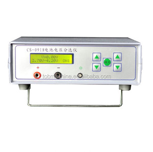
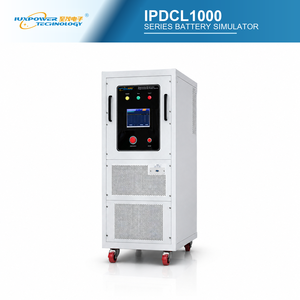
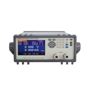
Our equipment line includes high-precision, bipolar programmable battery simulators (such as the IPDCL1000 and Aikesaibo ABS series), engineered with constant power function capabilities, current sinking ability, and ultra-fast dynamic response (<100 µs response time to 90% step load change). These simulators emulate real-world Lithium-Ion cell impedance chemistry, solid-state battery response curves, and solar array I-V profiles, enabling comprehensive system-level burn-in and efficiency profiling of GaN power modules.
Designed for absolute signal integrity, high-throughput manufacturing, and flexible OEM/ODM integration.
Optical isolation delivers >200 V/ns Common-Mode Transient Immunity (CMTI), eliminating ground loops and noise-induced gate faults during sub-nanosecond GaN switching events.
Patented microsecond voltage clamping measurement channels quantify dynamic $R_{DS(on)}$ degradation from 100ns to 10ms post-switch turn-on under full blocking voltages.
Planar busbar geometry and integrated high-frequency bypass capacitance minimize overshoot voltage spikes without distorting intrinsic device switching speeds.
Seamless integration with multi-channel battery cell simulators for full-loop testing of GaN-based BMS balancing, motor drives, and energy storage systems.
Comprehensive software suite supporting LXI, Ethernet, GPIB, Python SDKs, and LabVIEW drivers for effortless integration into high-speed automated production ATE racks.
Multi-zone high-speed thermal sensor arrays with automatic hardware interlocks prevent destructive thermal runaways during continuous power cycling stress tests.
As semiconductor fabs and power module original equipment manufacturers (OEMs) expand production capacities globally, procurement strategies for testing instrumentation are undergoing a fundamental transformation. Purchasing decisions are no longer driven solely by basic DC current/voltage ratings; rather, modularity, high throughput, dynamic accuracy, and automated integration are the primary operational metrics.
The electric vehicle industry is rapidly transitioning from standard 400V battery architectures to 800V and 1200V platforms to enable ultra-fast charging and higher drivetrain efficiency. While Silicon Carbide (SiC) currently dominates early 800V traction inverters, automotive-grade high-voltage GaN devices (Cascode and E-mode) are making substantial inroads into On-Board Chargers (OBC), DC-DC converters, and auxiliary drives due to lower gate charge ($Q_g$) and zero reverse recovery charge ($Q_{rr}$). Procurement teams must source test equipment capable of continuous stress testing up to 1200V with active thermal monitoring.
The proliferation of artificial intelligence compute infrastructure has surged power demands per server rack from 10 kW to over 100 kW. To maximize power usage effectiveness (PUE), server power supply units (PSUs) are upgrading to GaN-based Totem-Pole Bridgeless Power Factor Correction (PFC) topologies operating at 99%+ efficiency. Fabs require high-volume OEM automated test systems (ATE) capable of validating millions of GaN switches under high-frequency thermal stress before shipment.
Modern power networks require bi-directionality. GaN switches enable compact, highly efficient energy storage system (ESS) inverters. Testing these topologies requires bi-directional DC electronic loads and battery cell simulators that can instantaneously transition between sourcing and sinking current while monitoring semiconductor dynamic parameters in real time.
Why legacy curve tracers and standard DC test benches are inadequate for Wide-Bandgap device validation.
| Test Metric / Parameter | Legacy Silicon Test Equipment | Next-Gen OEM/ODM GaN Test Platform | Impact on Quality & Yield |
|---|---|---|---|
| $dv/dt$ Switching Speed | 10 V/ns to 30 V/ns | 150 V/ns to 200+ V/ns | Captures real-world switching stress without artificial damping. |
| Stray Loop Inductance ($L_s$) | 15 nH to 50 nH (Wired Fixtures) | < 1.8 nH (Planar Coaxial PCB) | Eliminates destructive voltage ringing & false over-voltage trips. |
| Dynamic $R_{DS(on)}$ Clamping | Not Supported (DC Static Only) | Active Nanosecond Clamping (100ns+) | Identifies electron trapping and current collapse before field deployment. |
| Gate Isolation CMTI | 20 V/ns to 50 V/ns Isolation | > 200 V/ns Fiber-Optic Floating Driver | Prevents gate driver latch-up and shoot-through failure modes. |
| System Integration | Standalone Manual Instruments | Full ATE Integration (SCPI, LXI, LabVIEW) | Dramatically reduces test cycle time in high-volume mass production. |
Over four decades of engineering mastery, vertical integration, and uncompromised quality assurance.
From precision CNC sheet metal fabrication and magnetic component winding to automated SMT surface-mount PCB assembly and final full-power burn-in testing, our entire manufacturing pipeline is unified under one roof. This strict vertical integration minimizes supply chain volatility and ensures total control over build quality and engineering tolerances.
No two semiconductor production lines are identical. We provide full OEM/ODM tailoring—including custom test fixture layout design, specialized socket cards, high-voltage matrix switches, tailored pulse timing algorithms, and branded customer UI software. Our modular architecture scales seamlessly from 1U benchtop systems to megawatt cabinet test bays.
Our core power electronics platform relies on a robust current-fed topology that utilizes inductive energy storage on the DC bus. This design offers inherent short-circuit protection, graceful handling of dynamic load transients, and superior reliability when driving highly capacitive or reactive loads compared to conventional voltage-fed power supplies.
As an established global exporter, we provide comprehensive international compliance certifications (CE, RoHS, ISO9001), customized international freight packaging, worldwide calibration traceability, and direct application support from experienced power electronics engineers rather than call centers.
Direct technical answers to common questions asked by procurement officers, test engineers, and lab managers.
Partner with a trusted OEM/ODM manufacturer to custom-build high-dynamic GaN dynamic parameter testers, double pulse test stations, or precision battery cell simulators tailored precisely to your operational requirements.
Get Catalog